VI
VI EN
EN
Why semiconductors need ESD corrugated plastic boxes
A semiconductor chip can fail from a discharge below 100 volts. Many devices react even sooner, with damage thresholds of only a few dozen volts. People cannot feel a discharge that small, yet a wafer or an IC fails instantly. For this reason, packaging inside a fab must control static from the very first internal move.
Corrugated plastic, also known as Danpla, coroplast, correx or corflute, is a hollow-core fluted PP sheet. When it carries a conductive additive, it becomes one link in the ESD control chain. As a result, ESD corrugated plastic boxes stay light, reusable, and compliant with the surface resistance limits the industry expects. Therefore this guide focuses on the technical numbers and on choosing the right box for each semiconductor step.
Static control requirements inside a semiconductor fab
The semiconductor industry classifies its parts as ESDS, meaning electrostatic-discharge-sensitive devices. In addition, the whole production area follows an ESD program, most often ANSI/ESD S20.20 or IEC 61340-5-1. Therefore any packaging that touches a component must sit inside that program and must never become a static source itself.
An ESD program covers more than boxes. In practice, it combines grounded workers, dissipative floors, wrist straps, and controlled packaging into one system. Consequently, a box only earns its place when its resistance matches the rest of that system. A single insulating container on the line can undo the whole chain.
Three surface resistance zones to know
Engineers rank ESD materials by surface resistance, measured in ohms. For example, the conductive zone sits below 1×10^5 ohms. The dissipative zone runs from 1×10^5 to 1×10^11 ohms. Above that range, a material acts as an insulator, so it charges easily and stays out of ESD areas.
Most boxes and partitions for semiconductors pick the dissipative zone. The reason is simple. Dissipative material lets charge bleed away slowly, which prevents a hard discharge that would damage a chip. Conductive material, in contrast, suits trays that ground a part quickly and directly.
How ESD damage happens
Damage arrives through two mechanisms. For example, the Human Body Model describes static from a person discharging through a part. The Charged Device Model, on the other hand, describes a part that charges itself, then discharges when it touches a grounded surface. Both events happen in a fraction of a second.
Latent failures are the greater risk. A mild discharge may not kill a chip at once, however it can leave a weak spot in the circuit. The part then passes outgoing tests, yet it fails early once it sits inside a finished product. As a result, the warranty and recall cost far outweighs the price of correct packaging.
Cleanroom environment demands
A fab runs inside a cleanroom. Therefore packaging brought in must shed few particles and release little outgassing. The sheet surface is smooth and free of fibers, unlike paper, so it keeps dust away from wafers. Moreover, the box has to survive routine alcohol wiping without losing its antistatic layer.
The material also has to be chemically clean. Virgin PP carries few impurities, and it releases little gas that could contaminate a wafer surface. For this reason, semiconductor packaging favors virgin resin over recycled plastic that may mix in contaminants.
Construction and materials of the boxes
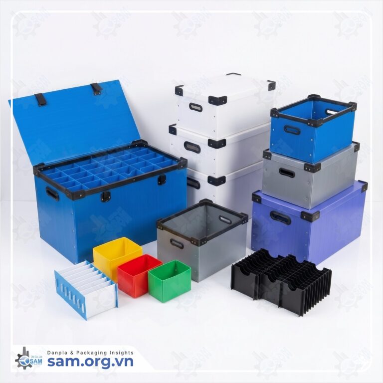
The box starts from a fluted PP sheet, typically 2 to 10mm thick depending on the load. In addition, its antistatic behavior comes from how the material is treated, and there are two main routes. Choosing the right route decides how long the ESD property survives in daily use.
Carbon-loaded versus coated sheets
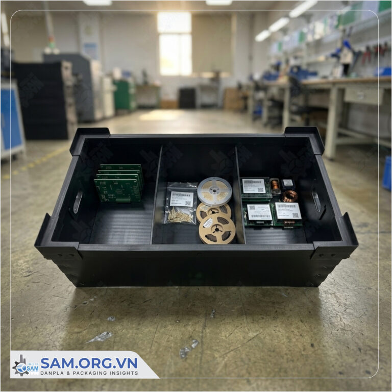
The carbon-loaded type blends conductive particles into the base resin, which gives it a signature black color. Because the ESD property lives throughout the material, it does not fade when the surface is scratched or wiped. Therefore this type lasts longest for boxes that circulate many times.
The coated type, by comparison, carries an antistatic additive on the outer surface. It costs less and comes in more colors. However, the coating can weaken with humidity and repeated wiping, so it fits short or medium life cycles rather than heavy reuse.
Partitions and matching accessories
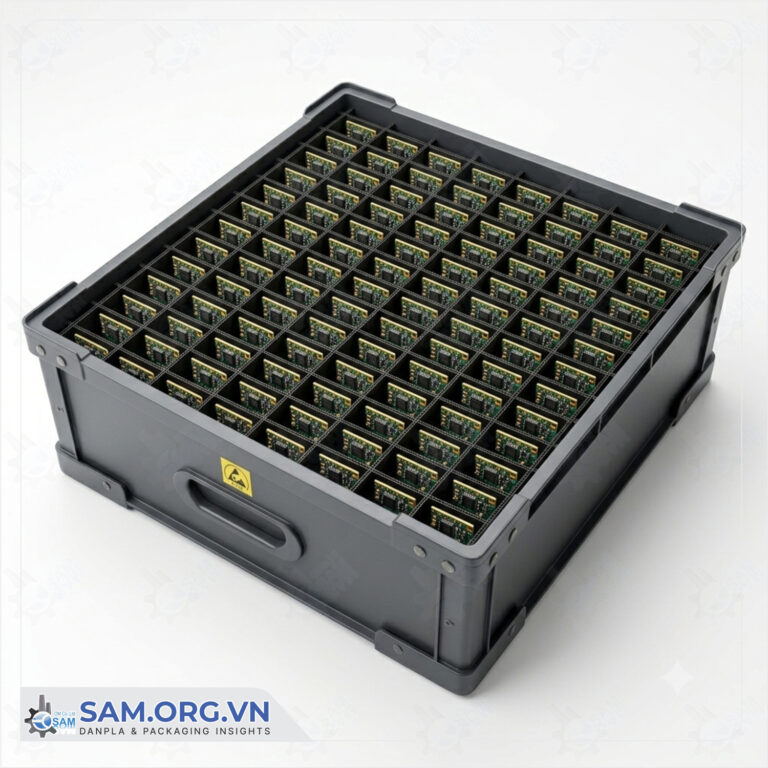
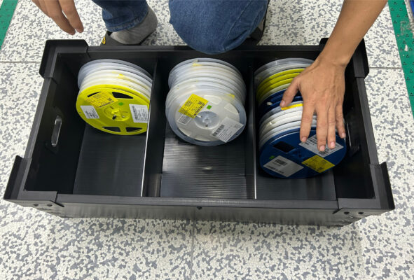
A semiconductor box rarely ships empty inside. Typically it holds partitions that split cells to the part size, so wafers or IC trays never knock against each other. Moreover, the partitions use the same ESD grade, which keeps the whole set uniform in resistance. Lids, handles, and corner strips then follow the same logic, because a single insulating piece would break the grounding path. For dividers alone, our ESD corrugated plastic partitions follow the same grade.
Verifying and holding the resistance grade
A resistance grade must be measured, not merely written on paper. Therefore the maker uses a surface resistance meter with two probes at a standard spacing, tested on a sample from each batch. In addition, the reading has to fall inside the customer range before a full run begins.
Coated resistance can drift with humidity. For this reason, many fabs add ionizers to neutralize charge on any insulating surface that remains. In short, the ESD box forms the base layer while the ionizer forms a second line of defense, so the two complement rather than replace each other.
Need technical advice tailored to your production line? Contact SAM’s engineering team — free, no obligation: +84 363 939 228 (Mr. Đạt)
Selecting the right box by semiconductor step
No single box fits every stage. Bare wafers, packaged ICs, and assembled boards each need different protection. Therefore the choice should start from the component, not from the box dimensions.
A quick way to start is to list four values: the part, its ESD sensitivity class, its weight, and its stacking height. With those figures in hand, the material grade, the thickness, and the divider layout follow logically. Therefore a short spec sheet up front saves several rounds of sampling later.
By component type and ESD sensitivity
A more sensitive part demands a tighter resistance zone. For example, wafers and reticles usually travel with dissipative partitions that avoid a hard discharge. Packaged ICs and boards, in contrast, often use a standard dissipative box with dividers. In practice, comparing the standard and antistatic corrugated plastic sheets helps you avoid ordering the wrong grade.
By load and stacking pattern
Sheet thickness follows weight and the number of stacked layers. For light loads such as IC trays, a 3 to 4mm sheet is usually enough. Heavier boards or tall stacks, however, need 5mm or more, plus reinforcing ribs on the walls and base. Moreover, the internal size should map to the pallet, so no space is wasted in storage.
Stack height also affects the lid choice. Tall stacks need a locking lid, so the load stays square under compression. Lower stacks can use an open box, which speeds loading on a fast line. Therefore the lid decision follows the stacking plan, not just the part itself.
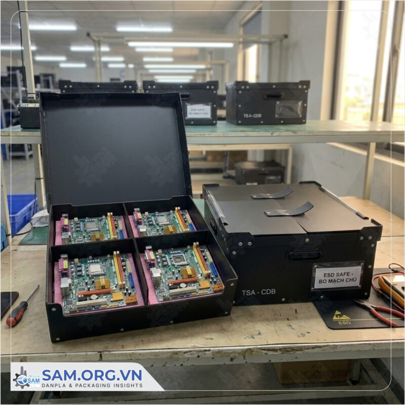
One detail is often missed, namely labeling. Therefore an ESD box should carry the ESD triangle symbol and a traceability code right on the wall, so operators never confuse it with a standard box on the same line.
Configuration examples by part type
A 300mm wafer cassette needs an outer box that holds the cassette firmly, with dissipative partitions that hug it so it cannot shift in transit. A JEDEC tray of ICs, for example, suits a shallow box with several dividers, stacking trays in layers. A large assembled board, by contrast, needs tall walls, reinforcing ribs, and a flat base for even support.
Foam inserts sometimes pair with the box for the most fragile parts. In this case, a dissipative foam layer cushions shock, while the fluted walls carry the load and the stack. Together they guard against both static and mechanical impact during handling.
For goods that travel between plants, the box should fold flat on the return trip. Moreover, the more cycles it completes, the lower the cost per trip becomes, which is the core advantage of reusable packaging over single-use boxes.
SAM’s capacity for ESD box production
SAM has produced fluted PP sheets and boxes since 2010, serving more than 300 clients across 15+ export markets. The antistatic line works closely with electronics and component makers, and the client page lists names such as Canon, Sumitomo Electric, and TENMA. Moreover, each ESD box is built to drawing, and it bundles partitions and accessories into one set of matching resistance. As a pillar reference, our corrugated plastic boxes and partitions page shows the base size and thickness range.
The process holds ISO 9001:2015 and ISO 14001:2015, and every batch is checked before it leaves the floor. For semiconductor work, the engineering team confirms the ESD grade against the customer specification and keeps it stable between batches. In addition, a sample is made and measured first, so a full run never starts on the wrong resistance grade. For electronics assembly more broadly, the same team also supplies corrugated plastic boxes for electronics.
Traceability matters as much as resistance in this sector. Therefore each batch can carry a lot code, so a quality issue traces back to a specific run. In addition, consistent labeling on every box lets operators sort ESD stock from standard stock at a glance.
Frequently asked questions
Is corrugated plastic the same as Danpla or coroplast?
Yes. Corrugated plastic, Danpla, coroplast, correx, and corflute all name the same fluted PP sheet. The terms differ mainly by region, however the material stays the same twin-wall board.
How does an ESD box differ from a standard one?
The difference lies in surface resistance. A standard box acts as an insulator, so it charges and discharges easily. An ESD box, in contrast, is carbon-loaded or coated, therefore its charge bleeds away in a controlled way within the dissipative or conductive zone.
Which resistance zone suits semiconductor parts?
Most steps choose the dissipative zone, from 1×10^5 to 1×10^11 ohms. This range lets charge drain slowly, which avoids a hard discharge. The exact grade should follow the ESD sensitivity of the part and the plant ESD program.
Can ESD boxes be used inside a cleanroom?
Yes. The surface is smooth and sheds fewer fibers and particles than paper, and it tolerates alcohol wiping. Moreover, the carbon-loaded type keeps its ESD property inside the material, so wiping does not remove it.